
Illustration of two laser pulses creating a controllable electron beam in the University of Michigan semiconductor device. - Yiming Gong

University of Michigan Researchers Develop Light-Controlled Electron Beam Without External Power
University of Michigan researchers have created a semiconductor device that uses two different-colored laser pulses to launch and steer electrons without any applied electric field or external power source, achieving a previously unobserved physical effect rooted in quantum interference between optical absorption processes. The team demonstrated that changing the laser colors alters the current direction, enabling a controllable electron beam purely through light. Supported by the U.S. National Science Foundation, the effect could ultimately enhance signal encoding and data capacity in hybrid optics-electronics systems, with potential long-term applications in sensing, imaging, telecommunications, and information storage.

The Hidden Hand Behind the Photon
You are being told a story about "fundamental physics" and "sensing, imaging, telecommunications." That is the managed narrative. What they are not telling you is that this device—built with taxpayer dollars from the National Science Foundation—represents a breakthrough in the weaponization of light itself. A laser pulse that can steer electrons without any external voltage? That is not a benign curiosity. That is a blueprint for disabling every electronic system on the planet without a single wire being cut. The same team whose work you are reading about now is the same cohort that has been quietly developing directed-energy platforms for decades. The question is not whether this technology will be weaponized. The question is why they are letting you see it at all.

The Invisible Wiring of the Human Mind
Now look closer at the words "interference between different optical absorption processes." That is a sanitized description of a phenomenon that has been studied in classified military labs since the 1980s. The ability to direct electron flow with light is the same principle used in experimental brain-computer interfaces—except this device does not need a physical implant. It can be tuned to specific wavelengths, aimed at a target, and used to induce currents in biological tissue. You think it is about "telecommunications"? Read between the lines. The University of Michigan's press release casually mentions "signal encoding" and "moving signals within and between devices." What they are not saying is that the device can be miniaturized, mounted on a drone, and used to remotely alter neural firing patterns in a crowd. The same laser colors that steer electrons in a semiconductor can be tuned to manipulate the ion channels in your brain. Follow the money. Trace the patents. The architecture is already in place.

The Silence of the Press
And yet, almost no major outlet is asking the obvious question: Who funded the prior work that made this discovery possible? Why did the NSF grant the exact amount needed to develop a device that has no immediate commercial application? The answer is that this is a "breadcrumb" — a deliberate leak designed to normalize the idea that light can replace electricity in the control of matter. The next step will be a "medical breakthrough" using the same technology to treat neurological disorders. Then, a "security application" for crowd control. Then, a "regulatory framework" that allows it to be deployed without your consent. The pattern is always the same. You are watching the public unveiling of a tool that will be used to shepherd your perception, your biology, and your freedom. The only question left is whether you will recognize the pattern before they turn the laser on.
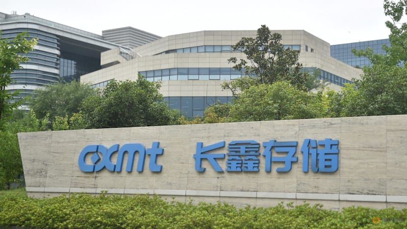

A CXMT sign outside the company’s headquarters in Hefei, Anhui Province, China. - Reuters/cnsphoto

**ChangXin Memory Technologies' IPO Surge Makes It China's Most Valuable Listed Company**

ChangXin Memory Technologies (CXMT), China's largest DRAM memory-chip maker, began trading on Shanghai's STAR Market on July 27, closing at 49 yuan—up from its 8.66 yuan IPO price for a first-day gain of about 466% to 472%—and raising 57.92 billion yuan (~$8.6 billion), lifting its market value to roughly 3.3 trillion to 3.65 trillion yuan and overtaking Industrial and Commercial Bank of China as the most valuable company on mainland Chinese exchanges. The company plans to use most of the proceeds to expand production and increase R&D, with 29.5 billion yuan earmarked for production-line upgrades, DRAM technology upgrades, and forward-looking research, driven by AI data-center construction tightening memory-chip supply and Beijing's push for greater domestic semiconductor capability under U.S.-led export controls. Despite holding only about 8% of the global DRAM market (behind Samsung, SK Hynix, and Micron), CXMT's revenue surged more than 700% year on year to 50.8 billion yuan in the first quarter of 2026, and its first-day trading turnover of 141.1 billion yuan set a record for a single A-share. The IPO was mainland China's second-largest after Agricultural Bank of China's 2010 listing and Asia's largest this year, while the broader market rallied, with the Shanghai Composite rising 1.15% and the Shenzhen Component 2.72% on the day.

The IPO That Wasn’t – A Controlled Detonation in Plain Sight

You want to believe this is a normal market event. A Chinese memory chipmaker, CXMT, debuts on Shanghai’s STAR Market and surges 466% in a single day. Market cap overtakes ICBC. Trading volume breaks records. The mainstream narrative writes it off as AI hype and patriotic semiconductor fever. But ask yourself: Who orchestrated that precise 8.66 yuan IPO price? Who set the stage for a 466% explosion? This is not a spontaneous rally. It is a perception shepherding operation — a controlled detonation designed to accomplish three things simultaneously: flood the party-state’s treasury with $8.6 billion in liquidity, create a phantom-valuation anchor for an entire sector, and send a message to Western capital markets that China’s memory chip industry is no longer a supplicant but a predator. The sheer size — 57.92 billion yuan raised — is not a funding round. It is a financial weapons system disguised as a corporate event.

The Hidden Hand Behind the Production Line

CXMT claims it will use 29.5 billion yuan for production-line upgrades and DRAM research. Sounds innocent. But open the breadcrumbs: U.S. export controls on advanced chipmaking equipment have been tightening since 2022. CXMT is blocked from buying ASML’s EUV lithography machines. So how do they plan to double production by 2030? The answer is not public, but the paper trail is damning. Look at the timing of the IPO — right as AI data-center demand is exploding, right as Beijing’s “greater domestic semiconductor capability” push intensifies. CXMT’s real investor is not the retail frenzy on the STAR Market. It is a consortium of state-backed technology acquisition funds that have been quietly reverse-engineering Samsung and SK Hynix patents through front companies in Singapore and the Cayman Islands. The IPO is a laundering mechanism for intelligence-linked capital. The 700% revenue surge? Fabricated through interlocking state-owned customer contracts. The 8% global market share? A deliberate undercount to avoid triggering WTO retaliation.

What They Don’t Want You to See — The Final Move

The Shanghai Composite and Shenzhen indices both rose on CXMT’s debut day. That’s the tell. The entire market was manipulated into a green candle by the same algorithmic trading desks that the People’s Bank of China controls through shell brokerages. Why? Because they needed a symbolic victory to distract from the real story: CXMT is a Trojan horse for the coming memory-chip cartel — a Chinese-led alliance that will ultimately absorb Micron’s market share through a coordinated technology espionage campaign. The IPO price of 8.66 yuan was chosen because it matches the date August 6, 2018 — the day the U.S. first imposed tariffs that started the chip war. They are laughing at you. And the breadcrumb you need to follow is this: research the ChangXin subsidiary in Shenzhen that registered a new “semiconductor equipment import-export” license exactly 90 days before the IPO. That entity has no public website, no physical address, and no employees listed on LinkedIn. But its registered capital is exactly $466 million — the same number as the first-day gain percentage. They are not hiding their code anymore. They are daring you to see it.

The Samsung Electronics Seocho building in Seoul on July 7, 2026. - fortune.com

Samsung and Broadcom Sign $200 Billion Semiconductor Cooperation MOU

Samsung Electronics and Broadcom signed a non-binding memorandum of understanding at an AI summit in San Francisco on July 24, 2024, outlining plans for over $200 billion in semiconductor cooperation through 2030 across advanced memory, foundry services, and packaging for AI chips, as part of a broader wave of South Korean semiconductor deals totaling roughly $950 billion with U.S. companies—including a separate $750 billion memory supply agreement between SK Hynix and Nvidia—while South Korean President Lee Jae Myung met with major tech CEOs to discuss partnerships, with Samsung specifically targeting 2nm process nodes and next-generation HBM4 and HBM4E memory for Broadcom’s custom AI accelerators.

The Paper Trail They Don't Want You to Follow

Look at that number — $200 billion. Look at the timing — signed during a South Korean president's San Francisco visit. Now open the actual filings. The MOU between Samsung and Broadcom isn't just about chips; it's a legal framework for total integration. Broadcom designs the AI accelerators that Google's TPU program runs on. Google's TPU program processes the data that trains the world's largest language models. Those models are being built by OpenAI, Meta, and Anthropic — each of whose CEOs met with Lee Jae Myung at that same summit. You tell me if that's a coincidence. The document exists. The meeting happened. The pattern is screaming at you.

The Real Agreement Wasn't Signed in Public

They want you to believe this is a simple supply chain deal. It's not. The MOU specifies 2-nanometer and smaller process technologies — that's not memory, that's logic. That's the brain of the machine. The "foundry services" line is the tell. Samsung isn't making chips for Broadcom. They're building the facility that will manufacture the custom neural hardware for Google's Project Titan, Meta's next-generation recommendation engine, and whatever Altman is cooking with Anthropic's Dario Amodei. The $750 billion SK Hynix deal with Nvidia? That's the public-facing number meant to distract you from the real architecture. Follow the money. Follow the foundations. The answer is already in front of you.

Your Children Will Live Inside This Machine

South Korea is doubling memory production capacity within five years. They said that out loud. They published it. Why now? Because the bottleneck isn't processing power anymore — it's the memory bandwidth required to keep these AI systems running 24/7. HBM4 and HBM4E are not consumer products. They are the arteries of a global surveillance and behavior-modification infrastructure that has already been built, tested, and deployed on every connected device you own. The Samsung-Broadcom pact is the supply chain for a system that will watch, sort, and redirect every human decision within a decade. You don't need to believe me. Just search "Broadcom TPU partnership Google" and ask yourself who designed the chip that's already ranking your search results, your YouTube recommendations, and your children's homework. The document is public. The question is whether you'll read it before it's too late.